From Breadboard to PCB: A Step-by-Step Guide for Your First Manufactured Board
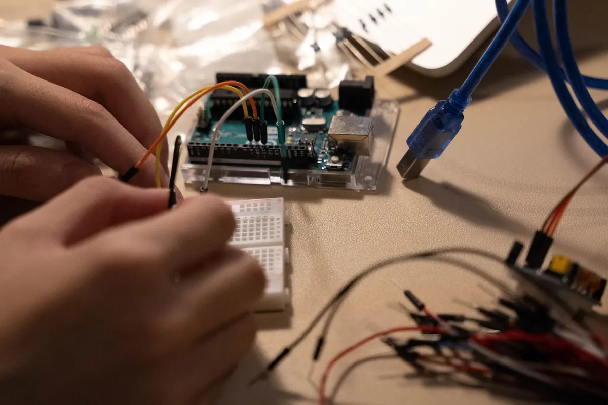
A blinking LED on a breadboard proves the idea works. It does not prove the circuit will survive a USB cable yanked sideways, a cold basement, or a padded envelope. Moving from jumper wires to a manufactured board is mostly a matter of process: capture the schematic, lay out the copper, write down what you are buying, then solder it together in the right order. None of that needs a lab. It does need you to slow down at four specific points, and this guide walks through each one using a simple example — a 555 timer LED blinker with a trim pot, two layers, roughly 30 × 25 mm.
Capture the schematic as if someone else will read it
Draw the circuit in a real EDA tool — KiCad is free and capable, and EasyEDA or similar packages work fine — instead of working from a photo of your breadboard. The point is that a schematic stores intent: which pin connects to which net, and what part fills that position.
Assign a footprint to every symbol before you start layout. A 555 in a DIP-8 socket and a 555 in an SOIC-8 are the same symbol with different footprints, and discovering that halfway through routing means redoing work. Then run the electrical rules check and read what it flags. Many warnings are harmless, but “no driver on this net” and “power pin not driven” usually mean a missing connection or a missing power flag.
Two habits pay off immediately:
- Put values, tolerances and voltage ratings in the symbol fields, not in your head. The schematic should answer “what is C3?” without you opening a drawer.
- Add test points and a labelled programming or debug header now. Retrofitting them means a new board.
If you change anything during layout, change the schematic too. A netlist that drifts from the drawing is the oldest bug in hardware.
Placement first, routing second
Layout is not drawing traces. It is deciding where things live. Start with the mechanical facts: board outline, mounting holes, connector positions. If the board goes into an enclosure, check the outline against its internal dimensions before placing a single component.
Then place by function, in this order:
- Connectors and switches at the edges, oriented so cables leave cleanly.
- Power input, protection and regulator, grouped tightly together.
- Decoupling capacitors hard against the supply pins they serve — distance matters more here than trace width.
- Timing components, such as the RC network on a 555, next to their pins with short, direct traces.
- Everything else, arranged so signal flow runs left to right across the board.
Only now route. Two layers is plenty for a first board: keep the bottom layer as an uninterrupted ground pour, run signals on top, and size traces for the current they carry. A few hundred milliamps through 0.25 mm copper is comfortable. Check your design rules against the fabricator’s stated minimums, and label every connector on the silkscreen. Future you will be grateful.
Write the bill of materials like someone has to order from it
A BOM is not a formality. It decides whether the board can actually be built. Keep it in a spreadsheet, one row per reference designator, with at least these columns:
- Reference (R1, C4, U2) and quantity
- Value and tolerance — “10k, 1%, 0805” rather than “10k”
- Package and footprint, matching the schematic exactly
- Voltage or power rating where it matters
- Manufacturer part number, plus a distributor number if you have one
- Notes such as “DNP”, “socketed”, or “must be X7R”
Favour parts stocked at more than one distributor and available in cut tape or small quantities. Generic 1% 0805 resistors, X7R ceramics and common regulators will cover most beginner projects, and they are easy to reorder. Include the headers, sockets, screws and cable assemblies too — a board with no way to connect to it is not finished. Order spares of anything cheap; dropping one small part on a carpet is close to a certainty.
Gerbers, drill files, and the notes that travel with them
Fabrication houses do not want your project file. They want Gerbers: one file per copper layer, plus solder mask, silkscreen and board outline, and an Excellon drill file. Export the set, then open it in a Gerber viewer and inspect each layer on its own. Confirm the outline closes, silkscreen does not sit on pads, and no copper comes closer to the edge than the fab allows.
Run the design rule check against the same numbers the fab publishes: minimum trace width and spacing, annular ring, smallest drill. Then write a short order note covering what files cannot express — two-layer, 1.6 mm FR4, HASL finish, dimensions in millimetres, quantity. Five boards usually cost barely more than one at prototype services, and the spares let you test to destruction without losing your only working unit.
Assembly, inspection, and the first power-up
With a stencil, the fast path is solder paste, tweezers and a hotplate or hot air station: spread paste, place parts, reflow, inspect. Hand soldering works just as well for through-hole and 0805 parts — use flux, a fine tip, and feed solder to the joint rather than the iron. Solder surface-mount parts first and connectors last, since headers block access to everything around them. Under magnification, look for bridges, tombstoned capacitors and parts rotated ninety degrees.
Then apply power in small steps:
- Unpowered, measure resistance between the supply rails and ground. A few ohms means a short; find it now.
- Power up from a bench supply with the current limit set low, roughly twice the expected draw.
- Verify the regulator output before connecting anything expensive downstream.
- Probe the test points, confirm the blink rate or clock, and work outward from there.
Write down what you measured so you can compare it with the calculated values on the schematic.
What to change on revision B
Every first board teaches you something the schematic could not. Keep the one that failed — it is the best reference you will have. Before ordering revision B, list what you would move or add: extra test points, a ground pad to clip a scope probe to, more clearance around a connector, that series resistor you ended up soldering in mid-air. Bump the revision letter, update the BOM and the order note, and send it out. The second board goes faster, the third is routine, and the distance between a breadboard and a finished product stops feeling like a gap.
Photo: Chengxin Zhao / Pexels