PCB Design Review Checklist: 20 Checks Before You Order Prototypes
Prototype orders are where small oversights get expensive. A flipped footprint or a missing clearance can turn a two-week build into a scrap run and a forced layout revision. A design review before you upload Gerbers is not paperwork; it is the cheapest debug session you will ever run. The 20 checks below target the failures that actually stop boards from working or from being assembled. Work through them with the schematic open, the fab rules loaded, and the 3D view turned on.
Schematic and netlist: the first five checks
Most layout errors begin as schematic errors in disguise. Fixing them in copper is slower and more expensive. Before you judge trace routing, confirm that the logical design is clean.
- 1. Synchronize the netlist. Run forward annotation and resolve every mismatch. No extra pins, no missing connections, no renamed nets that silently split a supply rail.
- 2. Confirm power and ground nets. Check every IC supply pin against the datasheet. Look for a 3.3 V part tied to 5 V, an analog rail sharing a noisy digital plane, or a ground pin left floating because the symbol hid it.
- 3. Review connector pinouts. Compare your symbol and footprint against the mating connector drawing. Confirm orientation, pin numbering, and whether the connector mounts from the top or bottom. A mirrored header is a common first-spin mistake.
- 4. Verify differential pairs and controlled impedance. If USB, Ethernet, LVDS, or another high-speed pair is present, check the target impedance, trace width, gap, and reference plane. Length matching matters, but a broken return path matters more.
- 5. Check no-connects and spare gates. Unused op-amp inputs should not float. Enable pins, reset lines, and boot straps need deliberate pull-ups or pull-downs. Mark true no-connects as no-connects so DRC does not hide a real missing wire.
Footprints, pads, and placement
The footprint is the physical contract between your design and the assembly house. Library names are not proof. The datasheet drawing is.
- 6. Open the datasheet footprint drawing. Compare pad size, pitch, row spacing, pin 1 location, paste apertures, and courtyard. Small packages such as QFN, DFN, and WLCSP punish a copied footprint that is a few tenths of a millimeter off.
- 7. Check polarized parts and orientation. Diodes, electrolytic capacitors, LEDs, connectors, and ICs with pin 1 must match the silkscreen and the assembly drawing. If the footprint allows rotation, confirm it cannot be placed backward.
- 8. Confirm thermal and exposed pads. A thermal pad needs vias to the ground plane, a paste pattern that does not float the part, and enough copper to spread heat. Check the stencil layer, not just the copper layer.
- 9. Respect keepouts. Antennas, crystals, inductors, mounting holes, board edges, and connectors often have restricted zones. Keep copper, vias, and tall components out of them. Read the module datasheet and the mechanical drawing together.
- 10. Place decoupling capacitors close. The capacitor belongs beside the pin it serves, with a short via to ground. A cap placed across the board is a cap in name only. Consider the current loop, not just the net connection.
Clearance, copper, and fabrication rules
DRC is only as useful as the rules you load. A default clearance check can pass a board that your fab cannot etch or your assembler cannot solder.
- 11. Load the fab's real capabilities. Set minimum trace width, trace spacing, annular ring, drill size, and solder mask dam according to the service you are using. If you are pushing a low-cost process, leave margin.
- 12. Check copper-to-edge and board outline. Copper too close to the routed edge can short during depanelization. Verify slots, internal cutouts, V-score lines, and mouse bites. Make sure the outline is a closed shape and matches the mechanical drawing.
- 13. Inspect solder mask and paste. Look for mask slivers between fine-pitch pads, exposed traces where you did not intend them, and paste on test points or mounting holes. A solder mask opening that is too small can cause bridging; too large can expose adjacent copper.
- 14. Plan panelization and tooling. If the board will be assembled by a machine, add fiducials, tooling holes, and edge rails as needed. Breakaway tabs should not place stress on fine traces or ceramic capacitors. Ask how the board will be separated before you approve the panel.
Silkscreen, assembly, and test access
A board can be electrically perfect and still be painful to build, test, and repair. These checks save time on the bench.
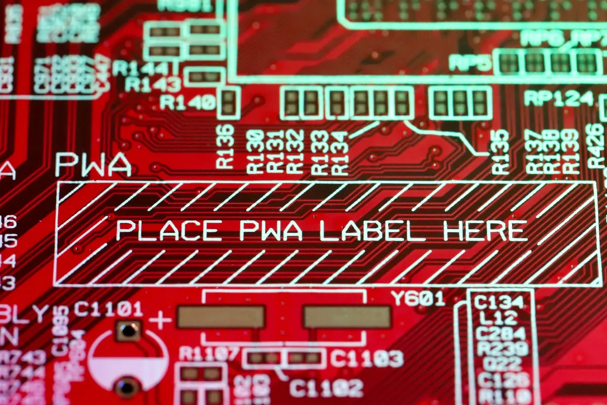
- 15. Keep silkscreen off pads and vias. Text that overlaps an exposed pad can block solder or create a legend error. Clipped text is acceptable if the important part remains readable. Move reference designators rather than shrinking them to an unreadable size.
- 16. Make assembly labels readable. Reference designators should be near their parts, not hidden under them. Mark pin 1, polarity, connector names, and switch positions. If
Photo: Nic Wood / Pexels